 |
|||
|
|
|||
|
Page Title:
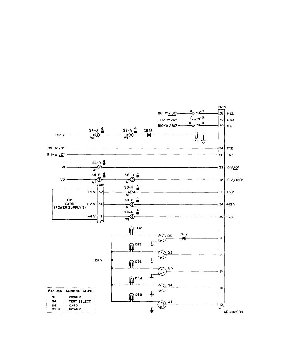
Figure 2-10. Comparator card A11 test functional diagram |
|
||
| ||||||||||
|
|
 TM 9-4931-363-14&P
voltage provides excitation for upper and lower tolerances
Reference voltage V6, in phase, from the wiper of R9 is
of out-of-phase comparators AR6, AR8, and AR10. Logic
connected to J9-24, and reference voltage V7, in phase,
excitation is provided as follows: +5 volts dc through wiper
from the wiper of R11 is connected to J9-16. Reference
1 and contact 5 of S8-F to J9-1; +12 volts dc through wiper
voltage V1, in phase, is connected through wiper 1 and
1 and S8-G to J9-34; and -6 volts dc through wiper 1 and
contact 7 of S4-D to J9-32. This voltage provides excitation
contact 5 of S8-H to J9-36. The input signals cause the
for upper and lower tolerances of in-phase comparators
comparator card to generate logic highs at J9-19, -16, -14,
AR2 and AR4. Refer to the A11 foldout schematic in TM
-8, and -6. The highs turn on, respectively, transistors Q6,
9-1270-212-14&P. Reference voltage V2, out of phase, is
Q2, Q3, Q4, and Q5 in the test set to light, respectively,
connected through wiper 1 and contact 7 of S4-E and
DS2, DS3, DS6, DS4, and DS5.
through wiper 1 and contact 5 of S8-D to J9-12. This
|
|
Privacy Statement - Press Release - Copyright Information. - Contact Us |