 |
|||
|
|
|||
|
Page Title:
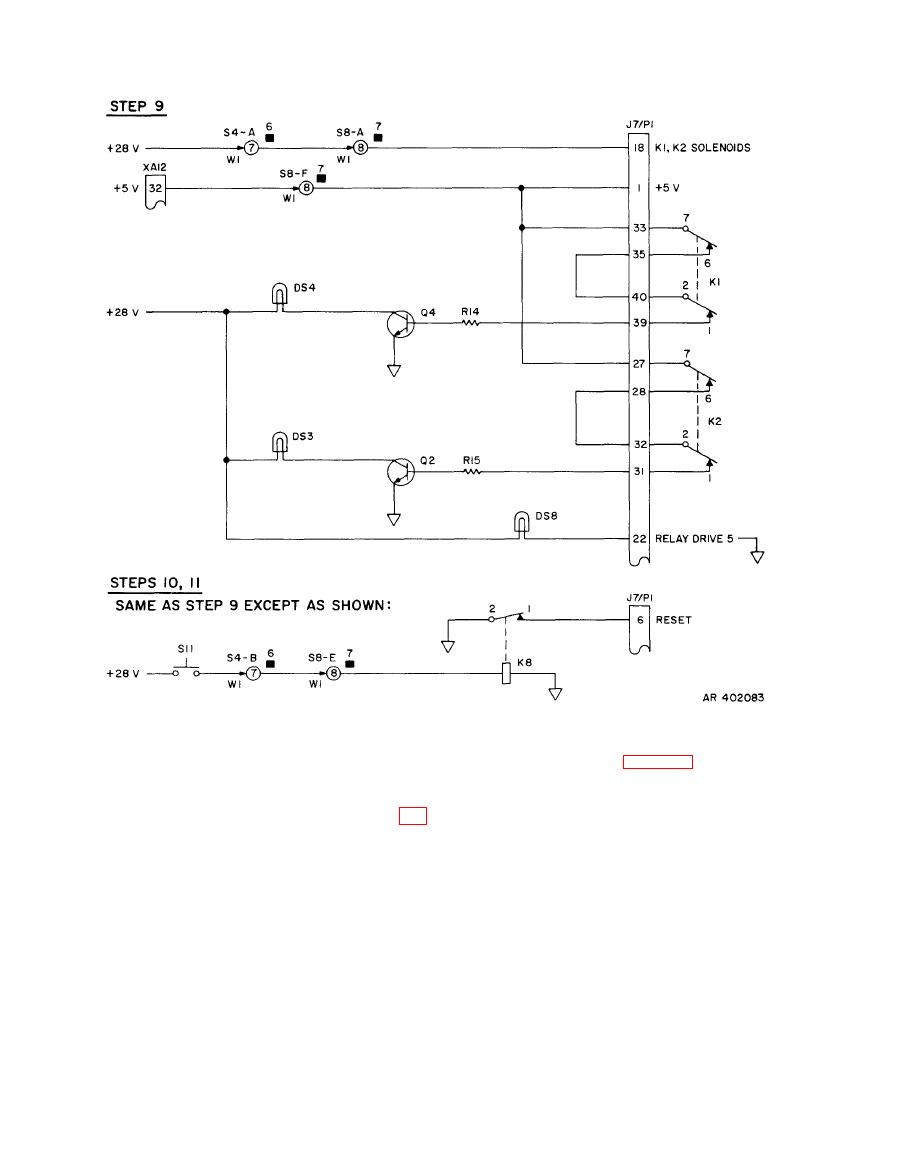
Figure 2-8. Sequencer card A9 test functional diagram (sheet 5 of 5) |
|
||
| ||||||||||
|
|
 TM 9-4931-363-14&P
Figure 2-8. Sequencer card A9 test functional diagram (sheet 5 of 5)
(2) Refer to step 1 in figure 2-9 and in the logic card
Logic-card-A10 or logic-card-A15 foldout
(2)
test table. The logic card under test is connected to J8 on
schematic diagram from TM 9-1270-212-14&P
the test set. Setting S4 to position 6 and S8 to position 1
connects 28 volts dc through wiper 1 and contact 7 of S4-A
(3) Logic card A10/A15 test functional diagram (fig.
and through wiper 1 and contact 2 of S8-A to J8-6 and -18.
2-9).
The test set provides a 28-volt return at J8-12. The 5 volts
dc is connected to J8-1 through wiper 1 and contact 2 of
NOTE
S8-F. The test set provides a signal return at J8-4. The -6
volts dc is connected to J8-16 through wiper 1 and contact
TM 9-1270-212-14&P information on logic card
2 of S8-H. Connector J8 in the test set connects J8-25 to
A15 differs basically only in that it has two
J8-37. Pressing S11 connects 28 volts dc through S11,
additional steps.
through wiper 1 and contact 7 of S4-B, through wiper 1
and contact 2 of S8-E to J8-9, the BIT initiate input. The
(1) To prepare for the logic card test theory
28 volts is connected from contact 2 of S8-E to energize
discussion, refer to the troubleshooting procedures for the
K8. Energized K8 applies a ground to J8-24. The 28 volts is
applicable logic card (A10 or A15) in TM 9-1270-212-14&P
also connected from contact 2 of S8-E through CR15 to
and mentally perform steps a through e .
2-44
|
|
Privacy Statement - Press Release - Copyright Information. - Contact Us |