|
| |
TM 9-254
4-17. Printed Circuit Board - Continued
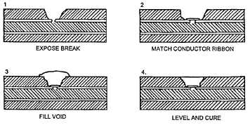
Figure 4-44.6. Damaged Conductor (Trace) Repair
(a)
Fill the void with a compatible epoxy mixture and allow to cure after the welding is completed.
(b)
Level the cured epoxy mixture with a chisel or mill to match the surface finish of the printed circuit board.
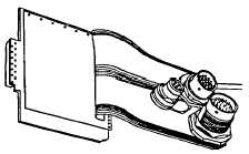
m. Flexible Circuits. Flexible circuits/cables are designed to provide efficient and practical methods for making
connections and utilizing space. The etched circuit is composed of flat copper conductors enclosed in insulating
materials The conductor to, Isolation bonding provides a barrier against moisture and gases, and is very durable. The
product may be bent, coiled, twisted, and formed to follow the various outlines of multiple systems. Assemblies may
be hinged, pulled-out and flexed for maintenance or inspection even when still in operation. Flex circuitry/cables
provide high reliability with less distortion or noise than conventional wiring. in addition, various methods can be used
for final assembly, such as, welding and soldering.
Figure 4-44.7. Flexible Circuit
l. Multiwire Technology. A multiwire PWA/PCB is a computer tape controlled series of conductor wires laid down on
an adhesive coated double-sided printed circuit board. The two sides of the board are used for voltage and ground
plane applications The voltage and ground planes are etched to both sides providing a semicured base for laying in
the conductor wires. The circuit is formed by using a pressure head, that imbeds the conductor wires in the adhesive.
Holes are then drilled in the board followed by the plating of these holes. Multiwire PWA/PCBs can be hand, wave, or
dip soldered using conventional soldering techniques. Multiwire printed circuit boards are recommended for high
frequency applications.
m. Additive Plating Technology. Additive plating may be defined in this manner: Additive plating is a process
whereby printed circuit boards are manufactured by selective depositing of a conductor material on an unclad base
material (no conductor material anyplace on the base material). The circuit is developed by applying a background
negative-image resist pattern, which leaves conductor areas and holes to be plated through, exposed for metal
deposit. Additive plating is an economy oriented process.
n. Leadless Components. A new trend in the manufacture of PCBs is to use so-called "LEADLESS COMPONENTS."
These are passive components such as resistors or capacitors which are made on semiconductor substrate material
and are greatly reduced in size. They do have axial leads, however, and are removed and replaced in a similar
manner to flat pack ICs (para 4-17.k.1). Use of leadless components can reduce a multilayer board to a single layer
and reduce its size by as much as one third.
4-46.4 Change 6
|