|
| |
TM 9-254
4-17. Printed Circuit Boards - Continued
(b)
Follow the foil repair procedure in (2) below.
(2)
Foil Repair Procedure.
(b)
Choose a matching foil, copper, aluminum, wrought copper, or gold ribbon.
(c)
Measure the conductor width and select the proper size for repair.
(d)
Cut foil length 1/4 inch longer than the break.
(e)
Prepare surface to be repaired by solvent or abrasion.
(f)
Lap reflow solder along the center of the conductor.
(g)
Inject epoxy filler under repair foil with a hypodermic needle.
(h)
Clean residue from the repair area.
(i)
Recoat the solder joint with conformal coating.
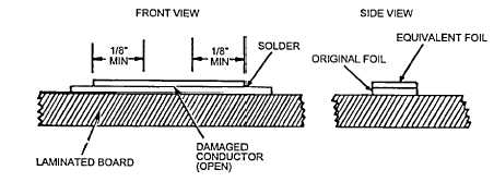
Figure 4-44.5. Foil Repair
(1)
Conductor Repair Procedures for Multilayer Boards. Use the parallel gap welding technique to repair defective
printed circuit conductors on double-sided and multilayer boards. This method can be used to repair breaks on both inner
and outer layers. Refer to the procedure below:
(a)
Locate break and chisel or mill away base until enough conductor is exposed to perform a weld (0.1 inch of
conductor on each side of the break)
(b)
Clean conductor to a shiny color for a proper weld.
(c)
Select a gold ribbon the same width as the conductor being repaired (preferred material).
(d)
Position gold ribbon over the break.
(e)
Apply a spot weld on each side of break with a parallel gap welder.
I
Control the interelectrode spacing for consistent results.
2 Vary the spacing according to the materials and the bond to be produced.
3 Fit the electrodes tight against the work for good electrical and thermal conductivity.
4 Use a spacing at least 1-1/2 times the thickness of the upper material.
Change 6 4-46.3
|